Abstract: An applicaTIon showing how the use of a microprocessor supervisor can be used to program a dual secTIon filter. Using the TIme delay from the reset circuit and strapping it to the power-fail comparator with a delay circuit, the filter can easily be programmed to provide the correct cutoff frequencies during power up using this reset circuit.
Certain dual-secTIon filter ICs have a common 7-bit port for programming the two cutoff frequencies (fC). If both sections require the same fC, you can strap an appropriate code to the port pins, but other applications require a different fC for each section. In such cases, a microprocessor is the obvious tool for sequentially programming the two filter sections, but lacking a µP, you can do the job without the circuit of Figure 1.
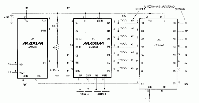
Figure 1. A µP-supervisory chip (IC1) directs the sequential loading of fC data into the dual, programmable lowpass filter IC2. The circuit reloads this fC data following each power-up.
IC2 is a continuous, dual-lowpass filter containing identical 2nd-order sections A and B. To program desired fC values, obtain corresponding codes from the data sheet and connect each pin of A0-A6 and B0-B6 to 5V ("1") or GND ("0") accordingly. (The latches internal to inputs D0-D6 remain "transparent" because inputs active-low WR and active-low CS are wired low.)
Latch IC3 also remains transparent because pin 11 is wired high. The latch outputs (1Q-7Q) are three-stated when the Output Control (active-low OC, pin 1) is driven high. When active-low OC is high, therefore, A0-A6 data drives the filter port (D0-D6). When active-low OC is low, B0-B6 data appears at the latch outputs and overrides A0-A6.
The µP-supervisory chip IC1, though normally used to monitor supply voltage and software execution in a µP system, generates directly usable signals for controlling IC2 and IC3: active-low RESET (pin 7), which remains low for 50msec after power-up, directs the input port of IC2 first to filter section A, then to section B. Active-low PFO (Power Fail Output, pin 5), which goes high in a few milliseconds after active-low RESET, provides a properly timed control signal for three-stating the latch outputs of IC3 (Figure 2).
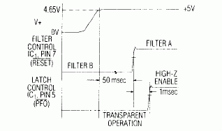
Figure 2. Timing relationships for the Figure 1 circuit.
The circuit as shown requires ±5V supplies. To operate on ±2.5V or on 5V alone, connect IC1's GND pin to the lower supply rail and drive IC2's pin 12 through a resistive divider (see MAX270 data sheet, Figure 3).