Abstract: This appnote explains how to communicate with the MAX6901 real-TIme clock (RTC) over a 3-wire interface.
The Maxim RTC (real-TIme clock) product family contains many parts that use a 3-wire serial interface for communicaTIon. This applicaTIon note describes the basics of the 3-wire interface and explains how it differs from other common serial interfaces. This should help you in simplifying the implementation of systems with RTCs that use the 3-wire serial interface.
Common Serial Interfaces for Communicating with RTCs
There are three common serial interfaces used to communicate with RTCs: SPI™ (serial peripheral interface, trademark of Motorola Inc.), I²C™ (trademark of Philips Corps.), and 3-wire (Dallas Semiconductor, Epson, Ricoh, Maxim, etc.).
Table 1. Comparison of Serial Interfaces
|
Bus
|
# Bus Pins
|
Signals
|
Signal Description
|
Bus Speed (Typical)
|
Data Format
|
| I²C |
2
|
SDA
|
Data in/out
|
100kHz to 400kHz
|
MSB first,
LSB last
|
|
|
SCL
|
Clock
|
|
|
| SPI |
4
|
DIN
|
Data in
|
1MHz to 10MHz
|
MSB first,
LSB last
|
|
|
DOUT
|
Data out
|
|
|
|
|
active-low CS
|
/Chip select
|
|
|
|
|
SCLK
|
Clock
|
|
|
| 3-Wire |
3
|
I/O
|
Data in/out
|
500kHz to 5MHz
|
MSB first,
LSB last
|
|
|
CS
|
Chip select
|
|
|
|
|
SCLK
|
Clock
|
|
|
The I²C interface requires only 2 wires for serial communication. There is more decoding of the states of SCLK and SDA to determine start and stop conditions than is required for SPI or 3-wire interfaces, where the active-low CS or CS line is active only when data transfers are occurring. For two-way data communication on the SPI bus, 4 pins are required. The 3-wire interface offers a simple implementation of a two-way data serial interface through a microcontroller's I/O port pins. The 3-wire RTC acts as a slave device, and the microcontroller acts as the master. The microcontroller (master) will control reading and writing to the RTC (slave) by providing the serial clocks and chip select as needed.
3-Wire Overview
All data transfers are framed by the CS signal, which must be active high for any data transfer to occur. At the beginning of any data transfer (rising edge of CS), SCLK should be low. This prevents the RTC from misinterpreting the transition of CS as a high-to-low transition of SCLK if SCLK were to be left high when CS transitions from a low to a high. Data is clocked into the RTC, through the I/O pin, on the rising edges of SCLK, and data is clocked out on the falling edge of SCLK. Data format is always LSB first to MSB last. In the "idle" state (CS low), the I/O line is high impedance.
3-Wire Single Byte Protocol
Figure 1 shows a Single Byte Read for the 3-wire serial interface. The first 8 bits sent after the CS is pulled high by the master comprise the Address/Command Byte, which tells the RTC if the data transfer is a read or a write and which register will be read to or written from. A typical RTC Address/Command Byte is shown below:
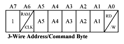
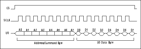
Figure 1. Single byte read.
For this Address/Command Byte, the MSB (A7) must be a logic "1". If it is zero, writes to the RTC will be disabled. A6 specifies clock/calendar data if logic "0" or RAM data if logic "1". A5-A1 specify the designated registers to be input or output, and the LSB (A0) specifies a write operation (input) if logic "0" or read operation (output) if logic "1". The command byte is always input starting with the LSB (A0). The Address/Command Byte is a write from the microcontroller (master) to the RTC (slave). Data for this write portion of the data transfer is clocked into the RTC on rising clock edges. On the eighth rising SCLK edge A7, the last bit of the Address/Command Byte is clocked into the RTC. After tCDH (CLK to data hold time, see Figure 5), the microcontroller must release the data line. On the eighth falling edge of SCLK, the RTC takes control of the data line and begins to output data.
The RTC outputs data on the falling edge of SCLK after tCDD (CLK to data delay time, see Figure 5). On the next rising edge of SCLK, the I/O pin will go to high impedance after tCCZ, which is specified with a maximum time. Minimum time for tCCZ can be 0nS. Because the I/O line can go to high impedance on the rising edge of SCLK, it is best to read the data from the RTC before the rising edge of SCLK but after tCDD (CLK to data delay time). This is accomplished best through the microcontroller I/O port pins by writing a low to SCLK, waiting tCDD (CLK to data delay time), reading the RTC I/O pin, and then writing a high to SCLK.
Figure 2 shows the 3-wire Single Byte Write. For this data transfer, the microcontroller has complete control of the RTC I/O line, which is configured as a data input. As with all data transfers, the Single Byte Write starts with an Address/Command Byte to tell the RTC that it is a write transfer and where the data is to be written. If more than 8 bits of data are written, only the first 8 bits will be written into the addressed register and the remaining bits will be ignored. If fewer than 8 bits are written before CS goes inactive (low), the data is ignored.
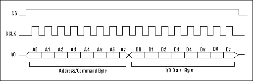
Figure 2. Single byte write.
3-Wire Burst Protocol
Figure 3 depicts the Burst Read operation for the 3-wire serial interface. In this mode, several successive bytes of data are read from the RTC. A distinctive Address/Command Byte is written to the RTC to indicate a Burst Read transfer and the starting address of the data. Data in consecutive addresses beginning with the starting address is read as long as CS is high and SCLK is still clocking.
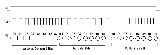
Figure 3. Burst read.
Figure 4 shows the Burst Write operation for the 3-wire serial interface. In this mode, several successive bytes of data are written to the RTC. A distinctive Address/Command Byte is written to the RTC to indicate a Burst Write transfer and the starting address of the data. Data in consecutive addresses beginning with the starting address is written as long as CS is high and SCLK is still clocking. If the microcontroller sends more data than will fit in a specific burst location, the burst counter in the RTC will wrap around and data in the original starting burst address will be written to again and so on.
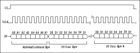
Figure 4. Burst write.
3-Wire Data-Transfer Timing Diagrams
Figures 5 and 6 show typical 3-wire data-transfer timing diagrams. In addition, Table 2 details typical specifications for the timing diagrams. Refer to the applicable RTC data sheet for detailed timing specifications for a particular device.
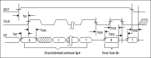
Figure 5. 3-wire read data transfer timing diagram.
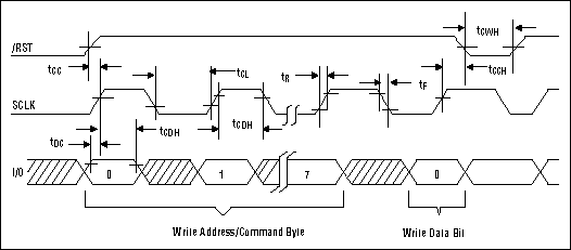
Figure 6. 3-wire write data transfer timing diagram.
Table 2. 3-Wire Serial Timing Specifications
(VCC = 2.0V to 5.5V, TA = -40 to 85C, unless otherwise noted. Typical values are at TA = +25°C.)
|
Parameter
|
Symbol
|
Conditions
|
Min
|
Max
|
Units
|
Notes
|
| Data to CLK Setup |
tDC
|
VCC = 2V
|
200
|
|
ns
|
1
|
|
|
VCC = 5V
|
50
|
|
|
|
| CLK to Data Hold |
tCDH
|
VCC = 2V
|
280
|
|
ns
|
1
|
|
|
VCC = 5V
|
70
|
|
|
|
| CLK to Data Delay |
tCDD
|
VCC = 2V
|
|
800
|
ns
|
1, 2, 3
|
|
|
VCC = 5V
|
|
200
|
|
|
| CLK Low Time |
tCL
|
VCC = 2V
|
1000
|
|
ns
|
1
|
|
|
VCC = 5V
|
250
|
|
|
|
| CLK High Time |
tCH
|
VCC = 2V
|
1000
|
|
ns
|
1
|
|
|
VCC = 5V
|
250
|
|
|
|
| CLK Frequency |
tCLK
|
VCC = 2V
|
|
0.5
|
MHz
|
1
|
|
|
VCC = 5V
|
DC
|
2.0
|
|
|
| CLK Rise and Fall |
tR, tF
|
VCC = 2V
|
|
2000
|
ns
|
|
|
|
VCC = 5V
|
|
500
|
|
|
| Active-low RST to CLK Setup |
tCC
|
VCC = 2V
|
4
|
|
µs
|
1
|
|
|
VCC = 5V
|
1
|
|
|
|
| CLK to Active-low RST Hold |
tCCH
|
VCC = 2V
|
240
|
|
ns
|
1
|
|
|
VCC = 5V
|
60
|
|
|
|
| Active-low RST Inactive Time |
tCWH
|
VCC = 2V
|
4
|
|
µs
|
1
|
|
|
VCC = 5V
|
1
|
|
|
|
| Active-low RST to I/O High Z |
tCDZ
|
VCC = 2V
|
|
280
|
ns
|
1
|
|
|
VCC = 5V
|
|
|
|
|
| SCLK to I/O High Z |
tCCZ
|
VCC = 2V
|
|
280
|
ns
|
1
|
|
|
VCC = 5V
|
|
70
|
|
|
Notes:
1. Measured at VIH = 2.0V or VIL = 0.8V for VCC = 5V; VIH = 1.4V or VIL = 0.6V for VCC = 2V.
2. Measured at VOH = 2.4V or VOL = 0.4V for VCC = 5V; VOH = 1.6V or VOL = 0.4V for VCC = 2V.
3. Load capacitance = 50pF.